Micro- and Nano-Fabrication
The best material is worthless if it cannot be processed, i.e. cannot be brought into the right shape or manufactured into a device. Research and development of new fabrication methods is, therefore, an important aspect in the development of novel nanostructured materials. At Empa we are developing micro- and nanofabrication technologies for the full range of existing materials including polymers, ceramics, metals, composites and fabrics.

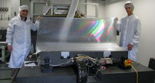
Excimer laser ablation system for micro-structuring very large areas up to 1900 x 1450mm2
- Lithography: Lithographic processes are applied to create patterns in a polymer film (resist) on a substrate. The dimensions of the desired structures and the to-be-patterned materials are important parameters to select between highest resolution (Electron Beam Lithography) for structures below 100nm. Through optical lithography we are able to produce patterns with sizes between 500 nm to several micrometers on very large surfaces, or 15 micrometer-sized structures on three dimensional substrates by a mask projection exposure system. To some extent, these techniques are available at Empa on laboratory tools. Alternatively, our research partners can carry out the lithography tasks on dedicated machines within cleanrooms available within the ETH Domain, for instance, in the Binnig Rohrer Nanotechnology Center at IBM Research in Rüschlikon, in ETH Zurich’s First lab and in CMI at EPFL.
- Self-assembly: Periodic structures are obtained by self-assembly of molecules, nanoparticles or nanocrystals. For example, we have developed in collaboration with colleagues from the Max Planck Institute in Mainz (D) a novel method to synthesize atomically precise and defect-free graphene nanoribbons (GNR) of only a few nanometers in width by molecular self-assembly. Polyphenylenes that possess halogens (bromine or iodine) at “strategically important” positions are used as building blocks. Depending on the geometry and the position of the linking sites, this process yields GNRs with different spatial structures (straight, chevron or bifurcated shape) and with two possible edge structures (armchair or zig-zag).
- Local removal of material: General ablative tools such as UV (wavelength = 355nm) pico-second pulse laser processing for micro-structuring of any material and deep UV (wavelength = 248nm) nano-second pulse laser surface structuring of polymers and ceramics with large surfaces (1.5 x 2 m2) are available at Empa. High resolution and precision ablative machining can be carried out with Focused Ion Beam (FIB) systems for structures with dimensions in the low nanometer range.
- Local deposition: With Focused Electron Beam-Induced Deposition (FEBID) we are able to deposit nano-sized metallic or semiconducting structures with tailored electrical, optical or magnetic properties from metal-organic precursors.

-
Share
